最近の成果: 薄膜のナノ形態制御と応用

-
-
★SERS基板,低反射ワイヤグリッド偏光子の実用化に貢献した.
-
➡SERS基板: ラマン散乱増強材
-
➡低反射WG偏光子: 液晶プロジェクタ.
-
-
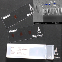
ニデック社から実用化されたSERS基板 Wavelet.
ソニーケミカル&インフォメーションデバイスから実用化された低反射ワイヤグリッド偏光子
-
3)M. Suzuki, W. Maekita, Y. Wada, K. Nakajima, K. Kimura, T. Fukuoka, and Y. Mori, "In-line aligned and bottom-up Ag nanorods for surface-enhanced Raman spectroscopy," Appl. Phys. Lett. 88 (20), 203121 (2006).
-
4)M. Suzuki, A. Takada, T. Yamada, T. Hayasaka, K. Sasaki, E. Takahashi, and S. Kumagai, "Low-reflectivity wire-grid polarizers multilayered by the glancing-angle-deposition technique," Journal of Nanophotonics 5, 011501-011509 (2011).
-
-
★Auナノ粒子をきっかけに成長する半導体や化合物ナノワイヤの成長が高温斜め蒸着によって加速されることを見いだした.
-
➡GeのVLS成長
-
➡O2雰囲気下でのGa2O3ナノワイヤの成長
-
-
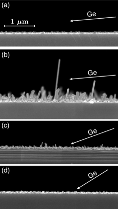
SEM images of the cross sections of (a) a Ge film deposited directly on the Si substrate at α=85° and samples deposited on a 5 nm thick Au catalyst substrates at the deposition angles of (b) 85°, (c) 73°, and (d) 58°. The arrows indicate the incident direction of Ge vapor.
-
2)M. Suzuki, K. Hamachi, H. Hara, K. Nakajima, K. Kimura, C.-W. Hsu, and L.-J. Chou, "Vapor-liquid-solid growth of Ge nanowhiskers enhanced by high-temperature glancing angle deposition," Appl. Phys. Lett. 99 (22), 223107-223103 (2011).
-
-
★局所プラズモン共振器による高効率光熱変換,光音響放出を実現した.
-
➡thermoplasmonicsへ展開
-
-
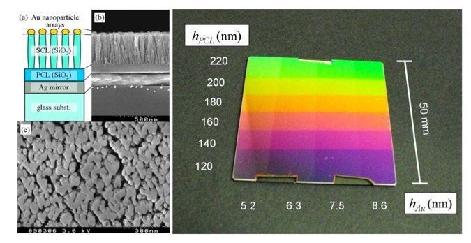
SEM image of a typical local plasmon resonator.
Visual appearance of local plasmon resonator chips
-
1)K. Namura, M. Suzuki, K. Nakajima, and K. Kimura, "Heat-generating property of a local plasmon resonator under illumination," Opt. Lett. 36 (18), 3533-3535 (2011).